The MAX8784 generates supply rails for the thin-film transistor (TFT) liquid-crystal display (LCD) panels in TVs and monitors. It includes a step-up regulator, a regulated positive and a negative charge-pump, three high-current operational amplifiers, and Dual Mode™, logic-controlled, high-voltage switch control block. HVS mode automatically increases the output voltages of the boost regulator and the positive charge-pump to stress test display panels during production. The MAX8784 can operate from input voltages of 4V to 5.5V and is optimized for LCD TV panel and LCD monitor applications.
The step-up DC-DC regulator provides a regulated supply voltage for TFT source drivers. The step-up regulator is a high-frequency (1.2MHz), high-efficiency, currentmode regulator. The step-up regulator has a built-in 110m(typ) power MOSFET. The high-switching frequency allows the use of ultra-small inductors and ceramic capacitors. The current-mode architecture provides fast transient response and easy compensation.
The step-up regulator features output undervoltage protection, soft-start, internal current limit, and adjustable output voltage by an external resistive divider.
The three operational amplifiers drive the LCD backplane and the gamma-correction-divider string. Each operational amplifier has a fast slew rate (45V/μs), a wide bandwidth (20MHz), and a high-output short-circuit current (200mA). Each op amp has rail-to-rail input and rail-to-rail output operation.
The positive charge-pump regulator and the negative charge-pump regulator provide regulated supply voltages for the TFT gate drivers. The positive charge pump is a two-stage charge pump, which requires no external diodes. The output voltages of both charge pumps are resistor adjustable. The logic-controlled high-voltage switch allows the manipulation of the positive TFT gate-driver supply.
The MAX8784 is available in a small (5mm x 5mm), lowprofile (0.8mm), 40-pin TQFN package and operates over the -40℃ to +85℃ temperature range.
MAX8784主要特性:
_ Step-Up Regulator Supply for LCD Panel Source Driver
Fast Transient Response to Pulsed Load
Built-In 18V, 4A, 0.11n-Channel Power MOSFET with Lossless Current Sensing
Cycle-by-Cycle Current-Limit Comparator 90% Efficiency (5V In to 15V Out)
1.2MHz Switching Frequency
_ Three High-Current 19V Operational Amplifiers
180mA Output Short-Circuit Current
45V/μs Slew Rate
20MHz Bandwidth
Rail-to-Rail Input and Output Operation
_ Regulated Charge-Pump Tripler with Integrated Diodes for TFT Gate-On Supply
_ Regulated Charge Pump for TFT Gate-Off Supply
_ Built-In Sequencing Internal Digital Soft-Start
36V Gate-On Switch
Startup Timing Capacitors for AVDD and GON
_ Undervoltage and Thermal Protection
_ 4V to 5.5V Input Operating Range
MAX8784应用:
LCD TVs and LCD Monitors
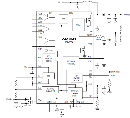
图1。MAX8784功能方框图
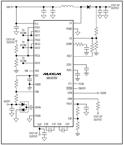
图2。MAX8784简化工作电路图

图3。MAX8784典型工作电路图
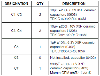
工作电路元件列表:
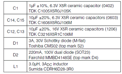

图4。MAX8784 HVS模式工作电路图
MAX8784评估板
The MAX8784 evaluation kit (EV kit) is a fully assembled and tested surface-mount PCB that provides the voltages and features required for active-matrix, thin-film transistor (TFT) liquid-crystal display (LCD) panels in LCD monitors and LCD TVs. The EV kit contains a stepup switching regulator, a two-stage positive charge pump for the TFT gate-on supply, a single-stage negative charge pump for the TFT gate-off supply, and three high-current op amps. Two capacitor-control delays are available: one to control the initial startup of the stepup, and the other to control the delay between the negative and positive charge pumps. Also included is a logic-controlled, high-voltage switch for the positivegate driver supply. A high-voltage stress (HVS) mode is provided to increase the step-up and the positive charge-pump output voltages for stress testing the display panel during production. A capa
citive dummy load is provided at the high-voltage switch output for ease of testing without a panel attached.
The EV kit operates from a DC supply voltage of +4.5V to +5.5V, as configured. The step-up switching regulator is configured for a +14V output providing at least 700mA. The positive charge pump is configured for a +28V output providing at least 50mA. The negative charge pump is configured for a -9V output providing at least 50mA. The three high-current op amps are each configured for a +7V output that can source or sink 180mA. The high-voltage switch can be controlled by external logic. The EV kit’s input voltage range can be lowered to +4V at slightly lower load currents.
The MAX8784 step-up switching regulator operates at 1.2MHz, allowing the use of tiny surface-mount components.
The MAX8784 thin QFN package (0.8mm max height), with low-profile external components, allows this circuit to be less than 3mm high.
MAX8784评估板主要特性:
♦ +4.5V to +5.5V Input-Voltage Range
♦ Output Voltages
+14V Output at 700mA (Step-Up Switching Regulator)
+28V Output at 50mA (Positive Charge Pump)
-9V Output at 50mA (Negative Charge Pump)
Three High-Current Op Amps (±180mA)
♦ 1.2MHz Switching Frequency
♦ All Output Voltages are Resistor Adjustable
♦ Logic-Controlled, High-Voltage Switch
♦ High-Voltage Stress Mode for the Step-Up and
Positive Charge-Pump Output Voltages
♦ Capacitor-Controlled Initial Startup Delay and Positive Charge-Pump Delay
♦ Low-Profile Surface-Mount Components
♦ Fully Assembled and Tested
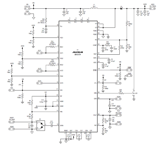
图5。MAX8784评估板电路图
MAX8784评估板元件列表:

The EV kit operates from a DC supply voltage of +4.5V to +5.5V, as configured. The step-up switching regulator is configured for a +14V output providing at least 700mA. The positive charge pump is configured for a +28V output providing at least 50mA. The negative charge pump is configured for a -9V output providing at least 50mA. The three high-current op amps are each configured for a +7V output that can source or sink 180mA. The high-voltage switch can be controlled by external logic. The EV kit’s input voltage range can be lowered to +4V at slightly lower load currents.
The MAX8784 step-up switching regulator operates at 1.2MHz, allowing the use of tiny surface-mount components.
The MAX8784 thin QFN package (0.8mm max height), with low-profile external components, allows this circuit to be less than 3mm high.
MAX8784评估板主要特性:
♦ +4.5V to +5.5V Input-Voltage Range
♦ Output Voltages
+14V Output at 700mA (Step-Up Switching Regulator)
+28V Output at 50mA (Positive Charge Pump)
-9V Output at 50mA (Negative Charge Pump)
Three High-Current Op Amps (±180mA)
♦ 1.2MHz Switching Frequency
♦ All Output Voltages are Resistor Adjustable
♦ Logic-Controlled, High-Voltage Switch
♦ High-Voltage Stress Mode for the Step-Up and
Positive Charge-Pump Output Voltages
♦ Capacitor-Controlled Initial Startup Delay and Positive Charge-Pump Delay
♦ Low-Profile Surface-Mount Components
♦ Fully Assembled and Tested
图5。MAX8784评估板电路图
MAX8784评估板元件列表: