<
/a>LED" title="LED">LED" title="LED">
LED驱动器采用LinkSwitchTM-PL系列LNK458KG,主要用于B10替代灯. 115 VAC输入48V输出时的效率大于86%,115 VAC输入96V输出时的效率大于87%,功率因素大于0.95,THD小于15%,起动时间小于300ms.本文介绍了LED驱动参考设计主要优势以及输出48 V/90 mA, 48 V/ 60 mA和96 V/ 45 mA参考设计主要指标,电路图和相应的材料清单.
4.3 W Power Factor Corrected LED Driver (Non-Isolated Buck Boost) Using LinkSwitchTM-PL LNK458KG
This document is an engineering report describing a non-isolated LED driver (power supply) utilizing a LNK458KG from the LinkSwitch-PL family of devices.
The DER-297 provides a single constant current output with an output power of 4.5 W.
The board can be easily configured for output voltages from 35 V to 100 V as shown in the example table below.
The key design goals were high efficiency and small size, enabling the driver to fit into candelabra and B10 sized lamps and maximize efficacy.
The board was optimized to operate over the low AC input voltage range (85 VAC to 132 VAC, 47 Hz to 63 Hz). LinkSwitch-PL based designs provide a high power factor (>0.95) meeting current international requirements.
The form factor of the board was chosen to meet the requirements for standard B10 LED replacement lamps. The output is non-isolated and requires the mechanical design of the enclosure to isolate the output of the supply and the LED load from the user.
The design was not optimized for operation with phase controlled (TRIAC) dimmers but this is possible with some modification will reduce efficiency.
The document contains the power supply specification, schematic, bill of materials, transformer documentation, printed circuit layout, design spreadsheet and performance data.
LED驱动参考设计主要特性:
Single-stage power factor corrected and accurate constant current (CC) output
Low cost, low component count and small PCB footprint solution
Highly energy efficient, >86 % at 115 VAC input for 48 V and >87 % for 96 V output
Superior performance and end user experience
Fast start-up time (<300 ms) – no perceptible delay
Integrated protection and reliability features
Single shot no-load protection / output short-circuit protected with auto-recovery
Auto-recovering thermal shutdown with large hysteresis protects both components and PCB
No damage during brown-out conditions
PF >0.95 at 115 VAC
%A THD <15% at 115 VAC
Meets IEC ring wave, differential line surge and EN55015 conducted E
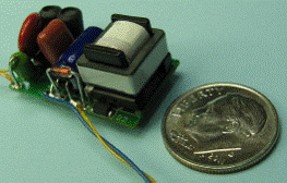
图1. LED驱动参考设计外形图
48 V, 90 mA参考设计指标:

48 V, 60 mA参考设计指标:
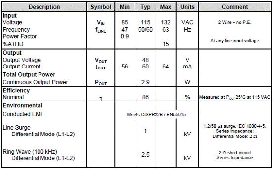
96 V, 45 mA参考设计指标:


图2.48 V, 90 mA参考设计电路图

图3.48 V, 60 mA参考设计电路图

图4.96 V, 45mA参考设计电路图
48 V, 90 mA参考设计材料清单:

48 V, 60 mA参考设计材料清单:
Make the following changes to modify the design from 48 V, 90 mA to 48 V, 60 mA.

96 V, 45 mA参考设计材料清单:
Make the following changes to modify design from 48 V, 90 mA to 96 V, 45 mA.

详情请见:
http://www.powerint.com/sites/default/files/PDFFiles/der297.pdf