
每个便携设备或者手持设备工程师都知道使功耗最小化是当前设计绝对需要的。但是,一个经验丰富的工程师就会明白微妙的细节可以使电池寿命延长到最大。这篇文章主要关注老练的专家怎样使用极低功耗的CPLD从嵌入式设计的I/O子系统里去挤出一点功耗。
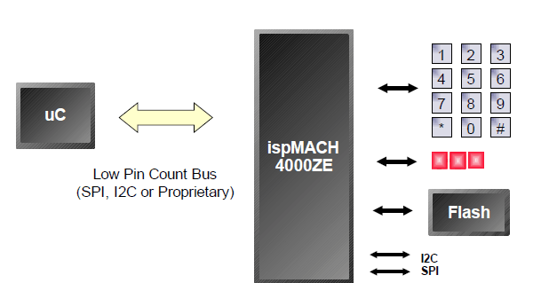
我们先回顾一下CPLD在嵌入式设计中一般被用来减少功耗和版大小,以及BOM成本。接下来,我们看怎样在待机模式下减少CPLD功耗,不只是小心选择设备,而且是选择一个合适的总线结构。我们在工作状态下的节能探索将包括选择逻辑门技术,智能I/O设计技术及精确电压供电管理技术。
Any engineer involved with portable or handheld products knows that minimizing power
consumption is an absolute requirement for today’s designs. But only the veterans
understand the subtle yet important details that can stretch a systems’ battery life to the
maximum. In this article we’ll focus on how those seasoned experts use ultra-low-power
complex programmable logic devices (CPLDs) to wring out every last microwatt from
the I/O subsystems of their embedded designs.
We'll begin by reviewing how CPLDs are commonly used to shrink power, board space and BOM costs in embedded designs. Next, we'll see how to minimize a CPLD's power consumption in its standby mode, not only by carefully selecting the device itself but also by choosing an appropriate bus parking scheme. Our exploration of power conservation during active operation will include techniques such as selective logic gating, smart I/O design and precision supply voltage management.
凡《网络安全与数据治理》(原《信息技术与网络安全》)录用的文章,如作者没有关于汇编权、翻译权、印刷权及电子版的复制权、信息网络传播权与发行权等版权的特殊声明,即视作该文章署名作者同意将该文章的汇编权、翻译权、印刷权及电子版的复制权、信息网络传播权与发行权授予本刊,本刊有权授权本刊合作数据库、合作媒体等合作伙伴使用。同时,本刊支付的稿酬已包含上述使用的费用,特此声明。
