
TOPSwitch-JX 系列TOP266EG是高性价比器件,它集成了725V 功率MOSFET,高压开关电流源,多模式PWM控制,振荡器,热关断电路,故障保护以及其它控制电路.265 VAC时无负载的功耗低于100 mW,工作频率132 kHz,降低了变压器尺寸和电源的体积.本文介绍了TOPSwitch-JX 系列主要特性,产品亮点,功能方框图,以及65W 19V和30W 12V通用输入反激电源电路图,27W LCD监视器电源参考设计主要指标,电路图以及所用材料清单(BOM).
Power Supply Using TOP266EG
90 VAC–265 VAC Input; 5V, 2.5A and 14.5V, 1A Outputs
Application LCD Monitor
TOPSwitch-JX cost effectively incorporates a 725 V power MOSFET, high voltage switched current source, multi-mode PWM control, oscillator, thermal shutdown circuit, fault protection and other control circuitry onto a monolithic device.
TOP266EG产品亮点:
• EcoSmart® - Energy Efficient
• Energy efficient over entire load range
• No-load consumption below 100 mW at 265 VAC
• Up to 750 mW standby output power for 1 W input at 230 VAC High Design Flexibility for Low System Cost
• Multi-mode PWM control maximizes efficiency at all loads
• 132 kHz operation reduces transformer and power supply size
• 66 kHz option for highest efficiency requirements
• Accurate programmable current limit
• Optimized line feed-forward for line ripple rejection
• Frequency jittering reduces EMI filter cost
• Fully integrated soft-start for minimum startup stress
• 725 V rated MOSFET
• Simplifies meeting design derating requirements Extensive Protection Features
• Auto-restart limits power delivery to <3% during overload faults
• Output short-circuit protection (SCP)
• Output over-current protection (OCP)
• Output overload protection (OPP)
• Output overvoltage protection (OVP)
• User programmable for hysteretic/latching shutdown
• Simple fast AC reset
• Primary or secondary sensed
• Line undervoltage (UV) detection prevents turn-off glitches
• Line overvoltage (OV) shutdown extends line surge withstand
• Accurate thermal shutdown with large hysteresis (OTP) Advanced Package Options
• eDIP™-12 package:
• Low profile horizontal orientation for ultra-slim designs
• Heat transfer to both PCB and heat sink
• Optional external heat sink provides thermal impedance equivalent to a TO-220
• eSIP®-7C package:
• Vertical orientation for minimum PCB footprint
• Simple heat sink mounting using clip provides thermal impedance equivalent to a TO-220
• Extended creepage to DRAIN pin
• Heat sink is connected to SOURCE for low EMI
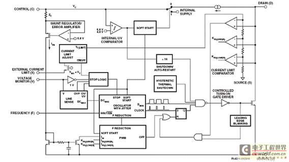
图1.TOP266EG 功能方框图(E和V封装)
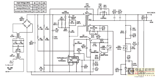
图2.采用TOP266EG的65W 19V通用输入反激电源电路图
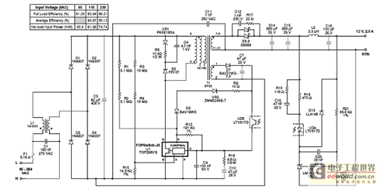
图3.采用TOP266EG的30W 12V通用输入反激电源电路图
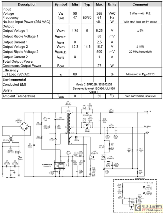
27W LCD监视器电源设计方案
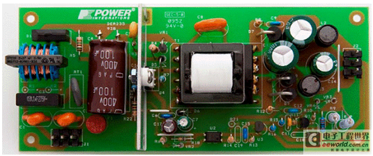
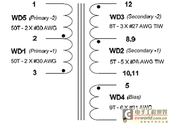
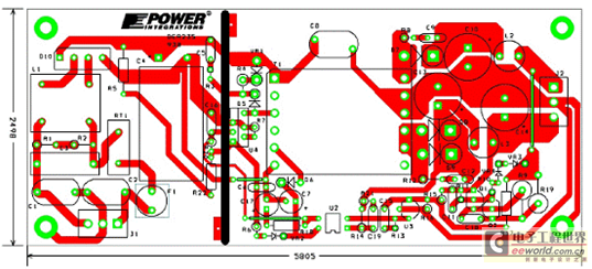
This document is an engineering report describing a 5 V / 2.5 A, 14.5 V / 1 A power supply utilizing a TOP266EG. The TOP266EG is part of the TOPSwitch-JX IC family from Power Integrations. The document contains the power supply specification, schematic, bill of materials, transformer documentation, printed circuit layout, and performance data.

凡《网络安全与数据治理》(原《信息技术与网络安全》)录用的文章,如作者没有关于汇编权、翻译权、印刷权及电子版的复制权、信息网络传播权与发行权等版权的特殊声明,即视作该文章署名作者同意将该文章的汇编权、翻译权、印刷权及电子版的复制权、信息网络传播权与发行权授予本刊,本刊有权授权本刊合作数据库、合作媒体等合作伙伴使用。同时,本刊支付的稿酬已包含上述使用的费用,特此声明。